4.11 Synchronization
In IQ sampling, phase errors introduce “crosstalk” between the I and Q components and degrade performance.
Timing (or clock) synchronizer
Carrier synchronizer
Phase is not always needed. In DPSK for example, only carrier frequency and symbol timing are required
4.11.1 Carrier recovery
Synchronous demodulation relies on the proper recover of the carrier at the receiver. For example, assume for simplicity that the baseband signal was upconverted at the transmitter via multiplication by a complex exponential , such that the transmitted signal is . Without loss of generality, the phase of the transmitter carrier is assumed to be zero, given that it serves as a reference to the other phases. In practice, the signal arrives at the receiver delayed by the channel propagation delay , but this is not important for this discussion and is assumed.
Ideally, the receiver can use to downconvert the signal and recover the signal of interest as indicated by:
However, the circuits that generate the sinusoids have imperfections, depend on the temperature, etc. Therefore, in practice, even expensive electronic components lead to some discrepancy between the carriers at the transmitter and receiver. Assuming the carrier generated by the receiver is , where is a phase offset that does not depend on and is the frequency offset (in rad/s). If this mismatch is not compensated, the signal at the receiver is
|
| (4.69) |
In this case, the effect is that is still shifted in frequency by a “carrier” composed by the frequency and phase offsets. The goal of carrier recovery is to estimate and then compensate these offsets, which in the current example would ideally consist of multiplying by .
Multiplication by a discrete-time complex exponential in digital domain is relatively easy. But when continuous-time sinusoids are used to implement the multiplication by , the frequency-conversion must be followed by a filtering stage to eliminate the extra spectrum replicas (or images). In this case, the filter(s) must be designed to avoid distorting the signal.
Another practical aspect is that receiver circuits, such as the one used in USRP’s daughter boards, can have an intermediate downconversion step, where an oscillator converts the RF signal (for example centered in 900 MHz) to an intermediate frequency (IF, for example, 70 MHz). This oscillator has its frequency chosen and then runs in “open loop”, i. e., its phase is not synchronized with the phase of the incoming signal . Again assuming for simplicity that a complex exponential is used, the mixer stage outputs the signal
This signal could then be digitized at the IF frequency or additional stages of downconversion (and filtering) used. Hence, it could be convenient to consider that is part of the frequency offset. In any case, the offsets and in Eq. (4.69) represent the (eventually accumulated) effects of the channel and receiver processing and compose the “carrier” to be estimated. The following paragraphs discuss the estimation of and using an FFT.
4.11.2 Carrier recovery using FFT
Some modulation schemes such as the commercial AM radio allocate power to the carrier, i. e., the PSD of the transmit signal shows a relatively large amount of power at the carrier frequency, as a spectrum line, and modeled with an impulse (see Figure 1.4). Alternatively, some communication systems such as the double-sideband suppressed carrier (DSB-SC) amplitude modulation, use a carrier to implement frequency upconversion but do not have spectral lines (impulses) at their carrier frequencies (see right-most PSD in Figure 1.2).
When the transmitter generates a signal with suppressed carrier, a trick to recover the carrier, which is still embedded in the modulated signal , is to process the signal via a non-linearity, such as squaring the signal. The squared signal can then be used as the input to a phase-locked loop (PLL), for example. A simpler example of carrier recovery, which uses FFT, is discussed in the sequel. A more advanced approach, using cyclostationary analysis was briefly discussed in Application 2.9.
PAM carrier recovery using FFT
Assume
PAM(t) is the transmitted signal and, for the sake of studying synchronization, the channel is ideal and is available at the receiver. The receiver then generates using a carrier that may have frequency and phase offsets with respect to the carrier used by the transmitter. Using trigonometry (Appendix A.2), can be written as:
|
PAM(t)
and the lower frequency replica is centered at
,
not at DC. The task here is to compensate both offsets and recover the signal
PAM(t)r(t) It is more effective to recover the carrier from than because, while may have a DC value PAM(t)] close to zero, the
new signal has discrete
spectrum components20
imposed by
. Using trigonometry again: Eq. (4.70) indicates that, depending on the values of
and
, it may be possible to filter
out all terms other than
using a bandpass filter. A numerical example is provided in the sequel. Example 4.21. Frequencies originated by squaring a PAM signal. A baseband signal with bandwidth BW when raised to the power of has its bandwidth expanded to . This can be seen by considering that multiplication in time-domain corresponds to convolution in frequency-domain, which expands the support of the original spectrum. Listing 4.17 provides an example of the frequencies obtained via Eq. (4.70) assuming a carrier frequency MHz (fc in the code) and a frequency offset of 27 kHz (fdelta), where these frequencies correspond to and fo, respectively. The PAM signal is assumed to have kHz. 1BWpam = 0.2; %signal bandwidth in MHz (200 kHz) 2fc = 900; %carrier frequency in MHz (900 MHz) 3fdelta = 0.027; %frequency offset in MHz (27 kHz) 4squaredBW = 2*BWpam; %BW expands by 2 after squaring 5%positive (negative freqs. not shown) center frequency of each term: 6f_DC=0+[-squaredBW, squaredBW] %DC frequency term bandwidth 7f_2wc=2*fc+[-squaredBW, squaredBW] %two times carrier frequency term 8f_2wcwoffset = 2*(fc+fdelta)+[-squaredBW, squaredBW] %3rd term 9f_4wcwoffset = 4*fc+fdelta+[-squaredBW, squaredBW] %4th term 10f_2woffset = 2*fdelta+[-squaredBW, squaredBW] %term of interest Listing 4.17 outputs:
     f_DC = [-0.4000    0.4000]
     f_2w0 = 1.0e+03 * [1.7996    1.8004]
     f_2w0woffset =  1.0e+03 * [1.7997    1.8005]
     f_4w0woffset =  1.0e+03 * [3.5996    3.6004]
     f_2woffset = [-0.3460    0.4540]
This indicates that the DC term
in Eq. (4.70) occupies a band from
to 400 kHz, overlapping with the term of interest
, which is located in the band from to kHz. The overlap can be a problem for a routine that estimates offsets. Hence, the receiver may impose a value distinct from to purposely have , where is the original PAM bandwidth, as discussed in the sequel. To avoid overlap, will be assumed to be
where is the actual (and unknown) offset to be estimated and is an intermediate frequency used by the receiver that can be chosen by the designer to avoid the mentioned overlap. The FFT-based estimation of frequency and phase offsets is simplified when three values are known (or can be estimated):
In order to choose , it is often possible to assume that . But choosing a large value for may be inconvenient, for example, if an ADC conversion should be used afterward. Fortunately, knowing , BW (assumed to be in Hz) and , allows to conveniently choose as follows. The angular frequency that will be used for the offsets estimation is within the range , i. e., the minimum search range is . Its minimum value should be higher than , to avoid overlapping with the “DC term” in Eq. (4.70). Besides, its highest frequency should be lower than . Hence, (in rad/s) can be chosen within the range
The following example illustrates the usage of Eq. (4.72). Example 4.22. Choosing the intermediate frequency for IF-based estimation of frequency and phase offsets. Listing 4.18 implements Eq. (4.72) to exemplify a possible range for . 1BWpam = 0.2; %signal bandwidth in MHz (200 kHz) 2fc = 900; %carrier frequency in MHz (900 MHz) 3fmax = 40/1e6*fc; %maximum absolute frequency offset in MHz (40 ppm) 4fIFmin = fmax + BWpam %minimum intermediate frequency 5fIFmax = 0.5*(fc - BWpam) - fmax %maximum intermediate frequency In this case the values of fIFmin and fIFmax were 236 kHz and 449.9 MHz, respectively. Choosing such extreme values is avoided because they could impose severe restrictions to filtering operations. The following example illustrates a complete FFT-based estimation procedure. Example 4.23. Complete example of frequency and phase offsets correction for PAM. Listing 4.19 illustrates the complete procedure for estimating the frequency and phase offsets corresponding to a PAM transmission In this example, the carrier frequency is GHz, the frequency offset is kHz ( rad/s) and the phase offset is rad. The intermediate frequency (fIF in the code) is chosen as 130 MHz. 6%% 0) Define simulation parameters and also check some choices 7fc=1e9; %nominal (transmitter's) carrier frequency in Hz (1 GHz) 8freqOffset=-500/1e6*fc; %frequency offset (-500 ppm) 9worstFreqOffset=(fc/1e6)*800; %worst accuracy is 800 ppm 10desiredResolutionHz=1/1e6*fc; %desired max error/FFT resolution,1 ppm 11%force freqOffset to coincide with a FFT bin via Rsym => Fs 12Rsym=desiredResolutionHz*1e4; %symbol rate in bauds (10 Mbauds) 13rollOff=0.5; %roll-off factor for raised cosine filter 14BWpam=(Rsym/2)*(1+rollOff); %PAM signal BW (~7.5 MHz if raised cos.) 15fIF = 130e6; %chosen intermediate frequency in Hz 16P=2; %power the signal will be raised to: x^P(t) 17phaseOffset=-0.3; %phase offset (to be imposed to the signal) in rad 18%choose a high enough sampling frequency to represent x^2(t): 19maxSquaredSignalFreq = 4*fc+fIF+worstFreqOffset+2*BWpam; 20L=ceil(3*maxSquaredSignalFreq/Rsym); % oversampling factor 21Fs=L*Rsym; %sampling frequency in Hz 22M=4; % modulation order (cardinality of the set of symbols) 23N=5000; % number of symbols to be generated 24fIFmin = worstFreqOffset + BWpam; %minimum intermediate frequency 25fIFmax = 0.5*(fc-BWpam)-worstFreqOffset; %max intermediate frequency 26if fIF > fIFmax || fIF < fIFmin 27 error('fIF is out of suggested range!') 28end 29if freqOffset > worstFreqOffset %based on accuracy of oscillator 30 error('freqOffset > worstFreqOffset') 31end 32%% 1) Transmitter processing 33%PAM generation: 34indicesTx = floor(M*rand(1,N))+1; % random indices from [1, M] 35constellation = -(M-1):2:M-1; % symbols ..., -3, -1, 1, 3, 5, 7,... 36m=constellation(indicesTx); % obtain N random symbols 37m_upsampled = zeros(1,N*L); %pre-allocate space with zeros 38m_upsampled(1:L:end)=m; % symbols with L -1 zeros in - between 39Dsym=3; % group delay, at rate Rsym (input symbols rate) 40p=ak_rcosine(1,L,'fir/sqrt',rollOff,Dsym); %square-root raised cosine 41%p=ak_rcosine(1,L,'fir/normal',rollOff,Dsym); %normal raised cosine 42gdelayRC=(length(p)-1)/2; %group delay of this even order RC filter 43sbb=conv(m_upsampled,p);%baseband: convolve symbols and shaping pulse 44n=0:length(sbb)-1; %discrete-time index 45wc=(2*pi*fc)/Fs; %convert fc from Hz to radians 46carrierTx=cos(wc*n); %transmitter carrier (assume phase is 0) 47s=sbb.*carrierTx; %upconvert to carrier frequency 48%% 2) First part of the receiver processing 49wOffset=(2*pi*freqOffset)/Fs; %convert freqOffset from Hz to radians 50wIF=(2*pi*fIF)/Fs; %convert fIF from Hz to radians 51carrierRx=cos((wc+wIF+wOffset)*n+phaseOffset);%Rx carrier w/ offsets 52r=2*s.*carrierRx; %downconvert to approximately baseband 53%% 3) Estimate and correct offsets: 54r_carrierRecovery = r.^P; %raise to power P 55%Will use at least desired resolution: 56Nfft = max(ceil(Fs/desiredResolutionHz),length(r_carrierRecovery)); 57if Nfft > 2^24 %avoid too large FFT size. 2^24 is an arbitrary number 58 Nfft = 2^24; %Modify according to your computer's RAM 59end 60if rem(Nfft,2) == 1 %force Nfft to be an even number 61 Nfft=Nfft+1; 62end 63minFreqOffset=P*(fIF-worstFreqOffset); %range for search using ... 64maxFreqOffset=P*(fIF+worstFreqOffset); %the FFT (in Hz) 65resolutionHz = Fs/Nfft; %FFT analysis resolution 66minIndexOfInterestInFFT = floor(minFreqOffset/resolutionHz);%min ind. 67maxIndexOfInterestInFFT = ceil(maxFreqOffset/resolutionHz);%max ind. 68R=fft(r_carrierRecovery,Nfft); %calculate FFT of the squared signal 69R(1:minIndexOfInterestInFFT-1)=0; %eliminate values at the left (DC) 70%strongest peak within the range of interest (start from index 1): 71[maxPeak,indexMaxPeak]=max(abs(R(1:maxIndexOfInterestInFFT))); 72estPhaseOffset=angle(R(indexMaxPeak))/P; %obtain phase in rad 73%R=[]; %maybe useful, to discard R (invite for freeing memory) 74estDigitalFreqOffset=(2*pi/Nfft*(indexMaxPeak-1))/P; %frequen. in rad 75estDigitalFreqOffset=estDigitalFreqOffset-wIF; %deduct IF 76estFrequencyOffset = estDigitalFreqOffset*Fs/(2*pi); %from rad to Hz 77%% 4) Demodulate and estimate symbol error rate (SER) 78%correct carrier offsets (taking in account the imposed wIF): 79carOffSet=exp(-1j*((estDigitalFreqOffset+wIF)*n+estPhaseOffset)); 80rc=r.*carOffSet; %generates complex signal with offsets subtracted 81rc2=2*real(rc); %convert to real signal, take factor of 2 in account 82rf=conv(p,rc2); %uses matched filter (note p is symmetric and real) 83startSample=2*gdelayRC+1; %take in account the filtering processes 84symbolsRx = rf(startSample:L:startSample+L*(N-1)); %extract symbols 85gain=sqrt(mean(abs(constellation).^2)/mean(abs(symbolsRx).^2)); 86symbolsRx = gain*symbolsRx; %normalize average energy of Rx symbols 87indicesRx=1+ak_pamdemod(symbolsRx,M); %add one to make 1,...,M 88disp(['SER = ' num2str(100*sum(indicesRx~=indicesTx)/N) '%']) %SER 89disp(['EVM = ' num2str(ak_evm(m, symbolsRx, 1)) '%']) Figure 4.46 and Figure 4.47 illustrate the baseband PAM signal and its frequency-upconverted version, respectively. 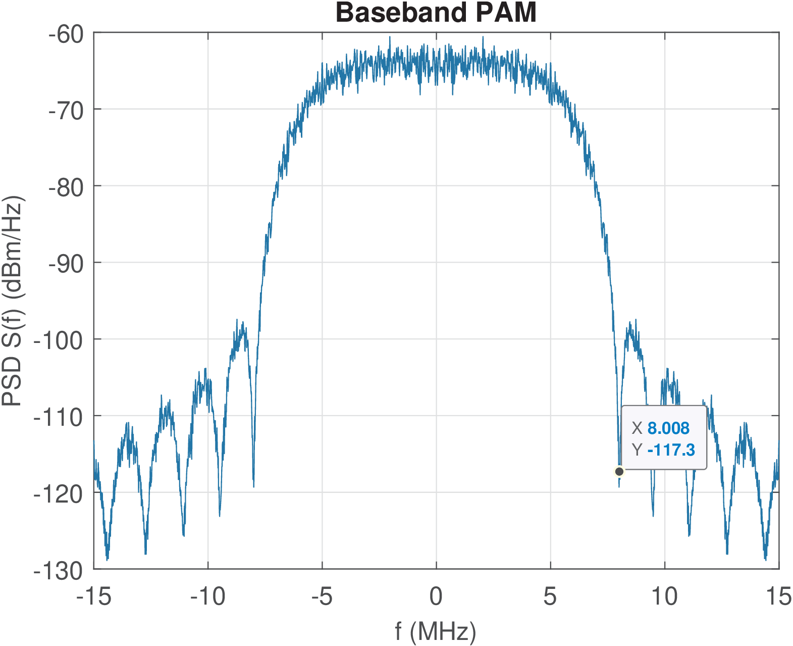
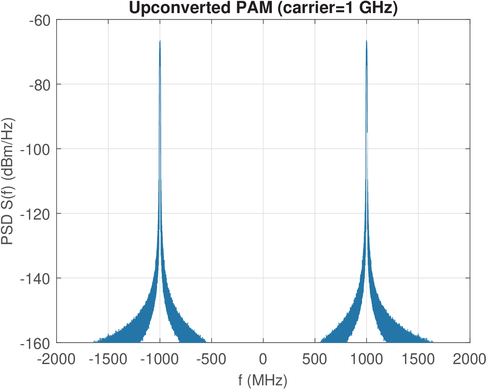
Figure 4.48 depicts the PAM signal after frequency-downconversion to an IF of 130 MHz for the estimation of the offsets. 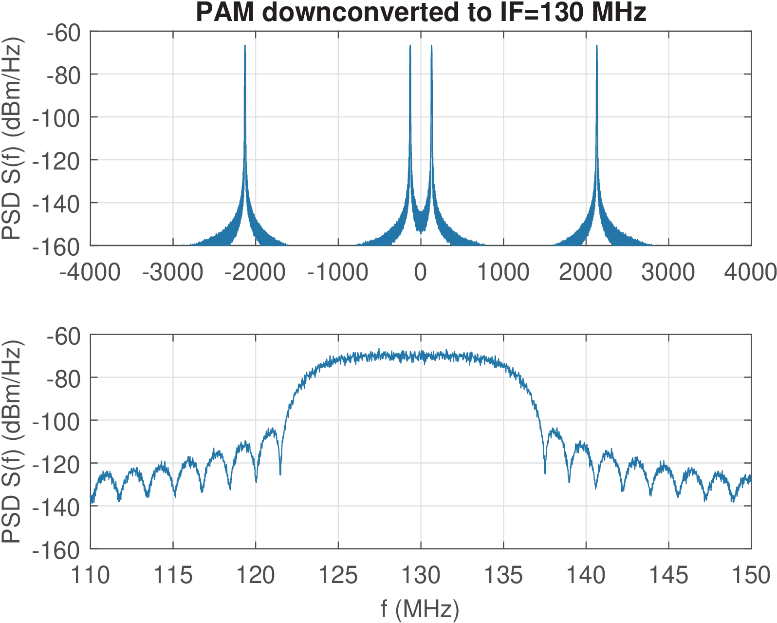
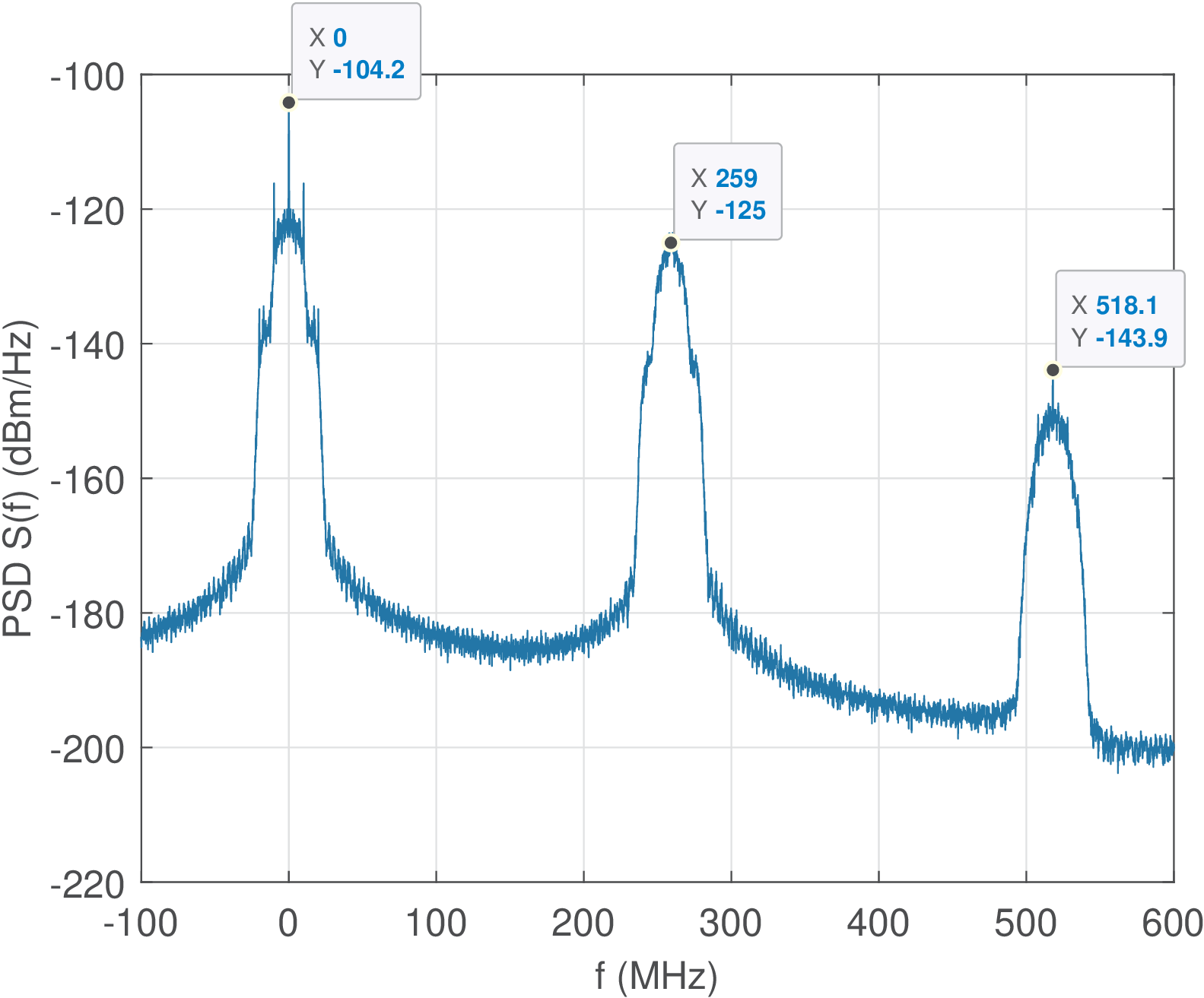
Figure 4.49 depicts the PSD of the signal used to estimate the offsets, which is obtained by squaring the received signal r. Note that the specific frequency in this case is 2*(fIF+freqOffset)/1e6=259 MHz (corresponding to rad/s), which is indicated in Figure 4.49 by a datatip. Note that a relatively high sampling frequency of Fs=12.44 GHz was adopted in this simulation in order to properly represent the squared signal. Care should be exercised when using smaller values of Fs in order to avoid aliasing. 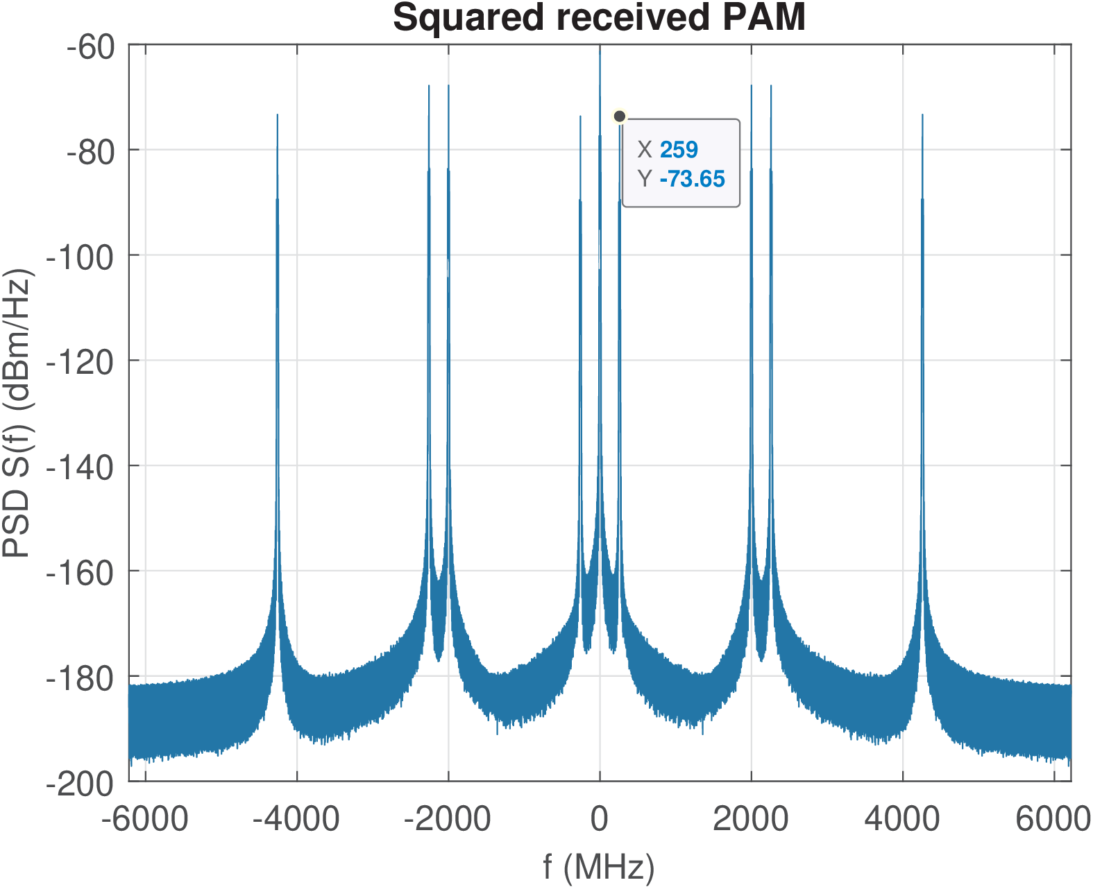
The squared received signal (whose PSD is in Figure 4.49) is converted by an FFT to the frequency domain. The values of range=minFreqOffset:maxFreqOffset indicate a search range of 258.4 to 261.6 MHz. As discussed, this range is centered at twice fIF (in this case 260 MHz) and has a band of 4*worstFreqOffset (3.2 MHz). Because in this example the FFT resolution is 1 kHz, the search range corresponds to the FFT indices minIndexOfInterestInFFT=258,400 to minIndexOfInterestInFFT=261,600. Within this range, the FFT index indexMaxPeak=259001 corresponds to the maximum absolute value. Figure 4.50 depicts 20*log(abs(R(range)))), which clearly shows the peak. The FFT value at this frequency (i. e., R(indexMaxPeak)) has a magnitude of approximately 6,200 and an angle of -0.6 rad. The magnitude value is not used but this angle allows to estimate the phase offset as rad. The frequency value corresponding to Mrad/s is obtained from indexMaxPeak as indicated in Listing 4.19. 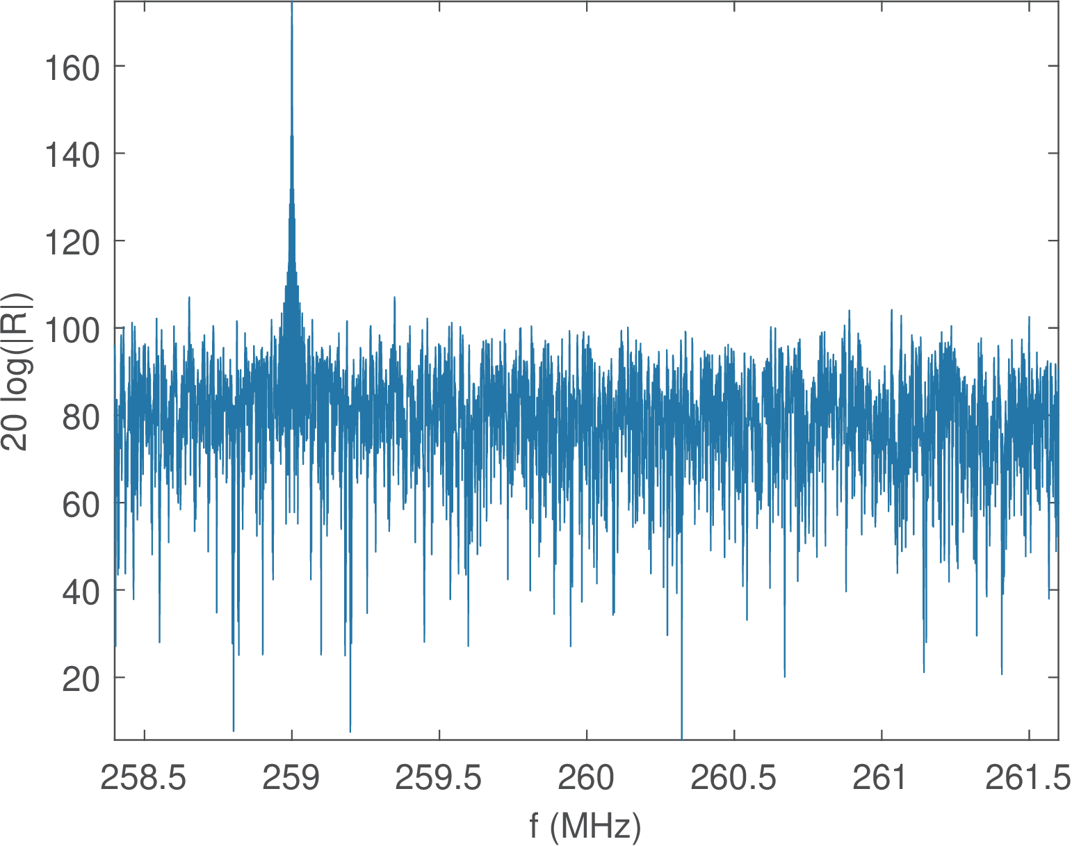
Having estimates of and , a complex exponential can be created and used to correct the offsets. The squared signal can be eventually discarded, because the next steps will depend on r. Figure 4.51 shows the PSD of rc, which is obtained by multiplying r by the mentioned complex exponential. 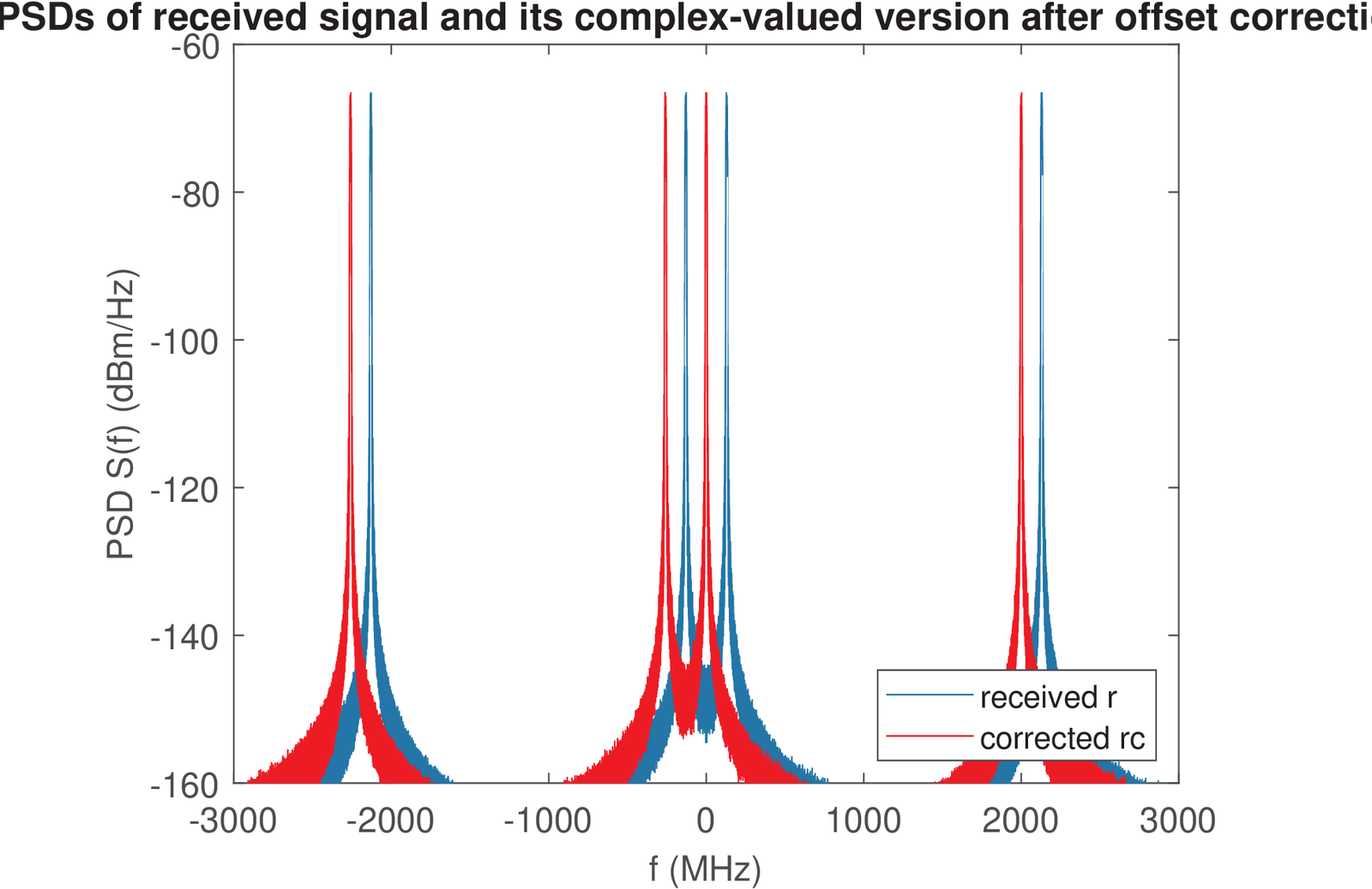
Figure 4.51 indicates that rc is complex-valued because its PSD does not have Hermitian symmetry. Discarding its imaginary part leads to the signal with PSD depicted in the top plot of Figure 4.52. This signal is then matched-filtered using the same square-root raised cosine (SRC) adopted by the transmitter, and the final signal is rf, with PSD showed in the bottom plot of Figure 4.52. 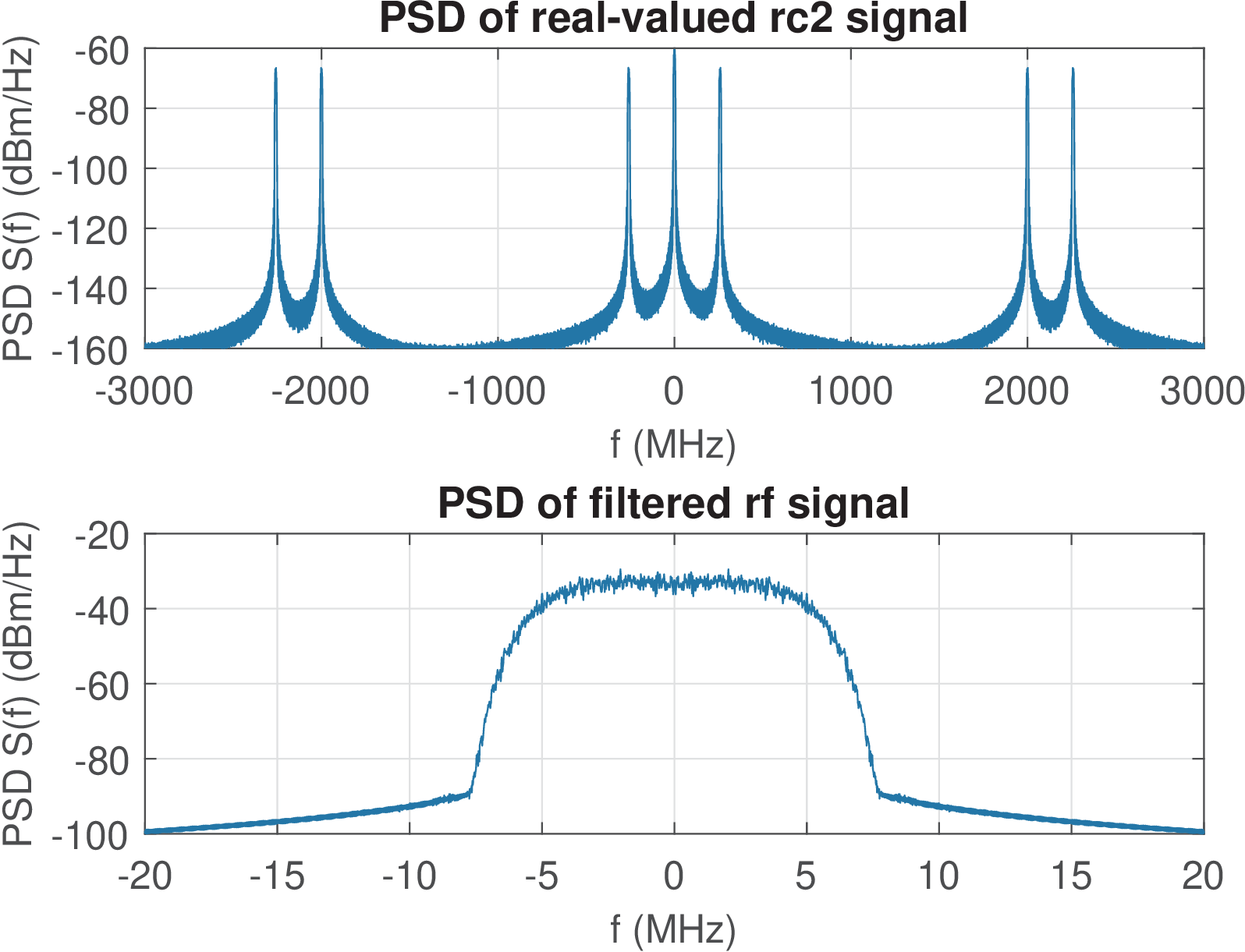
The adopted SRC has a group delay of gdelayRC=3,732 samples. Taking in account the two filtering stages (at transmitter and receiver), the first symbol is extracted at sample startSample=2*gdelayRC+1. The final received symbols constellation is depicted in Figure 4.53. 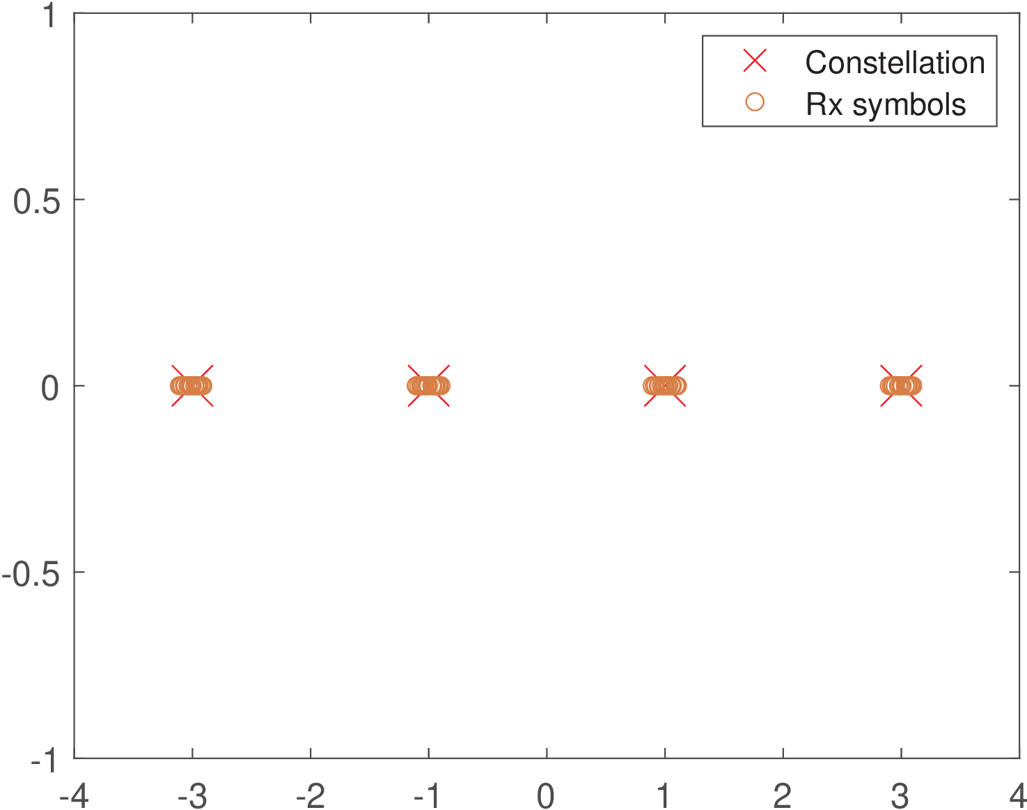
In this simulation, the SER was 0% (no symbol errors) and the EVM = 1.94%. Example 4.23 illustrated a “perfect” estimation, but there are several difficulties related to this FFT-based procedure. For example:
The latter issue and the high-computational cost of the FFT-based method motivate the adoption of adaptive algorithms, such as the ones based on the PLL. Before discussing them, the FFT-based method is applied to QAM in the sequel. QAM carrier recovery using FFTThe offsets estimation procedure used in Listing 4.19 is based on the discrete spectrum
component
that appears in Eq. (4.70). The implicit condition for having this component available for the
estimation is that
, which is a consequence of having , where is the PAM constellation symbol. As discussed in Appendix A.18.2, some QAM constellations (called here “balanced”) lead to , where is the transmit signal, and a discrete spectrum component would not be created. In such cases, a power of is used to create as the input to the FFT. The reader is invited to vary the modulation order and to evaluate, for example: 1M=16; m=ak_qamSquareConstellation(M); mean(m.^2) %returns 0 2M=16; m=ak_qamSquareConstellation(M); mean(m.^3) %returns 0 3M=16; m=ak_qamSquareConstellation(M); mean(m.^4) %it's not zero With a similar test, it can also be seen that, for a modulation order (which corresponds to a “rectangular”, not “square” constellation), and, in this specific case, would work. But in other cases is required. This choice makes a little more complicated the FFT-based offsets estimation, as discussed in the sequel. A QAM receiver uses both a cosine and sine to recover the in-phase and quadrature components, but the offsets estimation procedure is illustrated here with just the cosine. The transmit QAM signal is and (again considering an ideal channel) the receiver then generates (and it is assumed here that ). It is the analysis of that will lead to the estimation of and . The Matlab Symbolic Math Toolbox can be used as follows: 1syms xi xq wt Dt p %define symbolic variables and calculate: 2simplify(expand(((xi*cos(wt)-xq*sin(wt))*cos(wt+Dt+p))^4)) where Dt corresponds to , p to , etc. This allows to decompose in 54 parcels that after careful inspection can be written as: The (real-valued) signal centered at DC is given by , and has a bandwidth expanded by approximately times the one of the original QAM signal. The other signals and are described in Table 4.4.
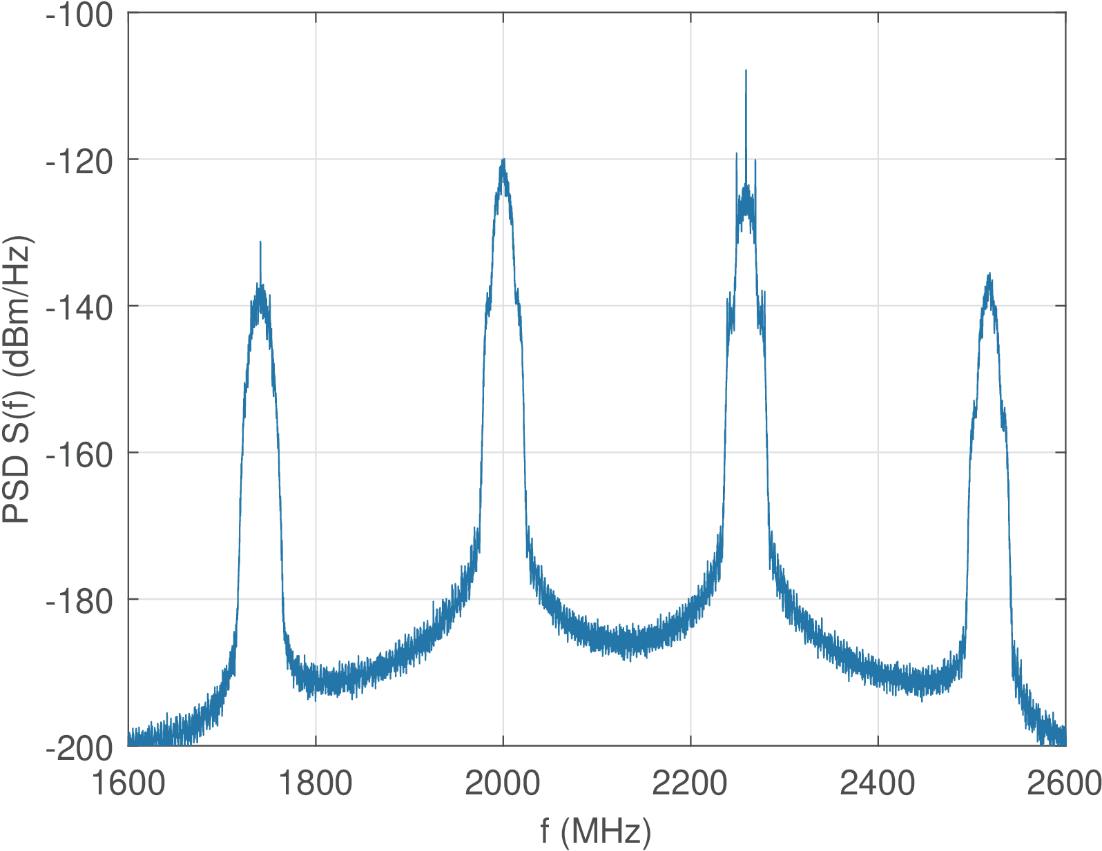
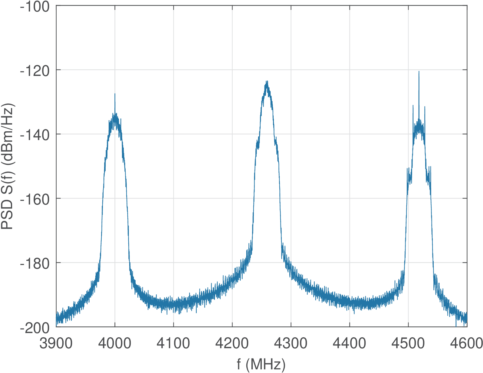
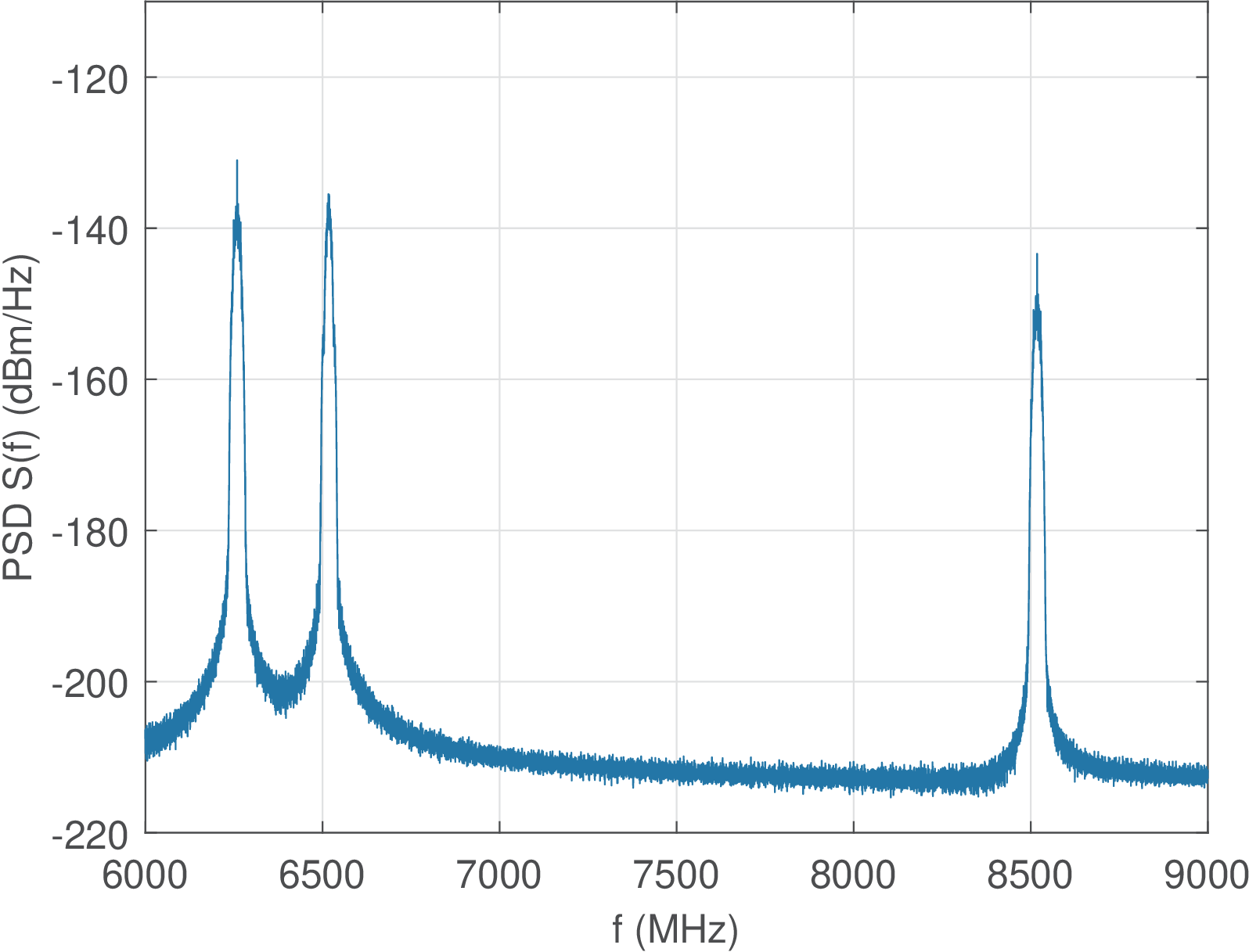
Some frequency values of interest in Eq. (4.73) are: , and , which correspond to the three lowest frequencies above DC. The term of interest to be used to estimate the offsets is , which centers the signals and at frequency rad/s. The highest center frequency is associated to the term . The other frequencies can be found in snip_channel_qam_squared_freqs.m. As expected, the signals in Table 4.4 depend on the PAM signals and . To better understand why some of these signals do not present a discrete spectral line (as indicated in the last column of Table 4.4), it is useful to simplify the discussion assuming that the continuous-time signals are perfectly sampled at the symbol rate such that, for example, instead of statistical moments of continuous-time signals such as , one can deal directly with the associated constellation symbols and their moments. Because we are interested in balanced QAM constellations, assume that the two underlying PAMs have the same order . In this case, the signal sampled at has an average value of because , where and are the PAM transmit symbols. Similarly, the average of at the baud rate is because and are independent, such that e. g. because . In contrast, has a non-zero average dictated by . Along this reasoning one can explain the presence of a spectrum line for and the absence for as indicated in Table 4.4, for example. A numerical example that further discusses these relations is provided in the sequel. Example 4.24. Complete example of frequency and phase offsets correction for QAM. The companion script MatlabOctaveBookExamples/ex_fftBasedQAMCarrierRecovery.m is similar to Listing 4.19 but incorporates some modifications to support offsets estimation for balanced QAM constellations, restricted to a phase offset rad due to the inherent phase ambiguity created by the process of raising the signal to the fourth-power. Figure 4.54 depicts the PSD of , obtained via Eq. (4.73). In this case, snip_channel_qam_squared_freqs.m informs that the 12 frequencies related to are: 0.259, 0.518, 1.741, 2.0, 2.259, 2.518, 4.0, 4.259, 4.518, 6.259, 6.518 and 8.518. respectively, all in GHz, as can be identified in Figure 4.54. 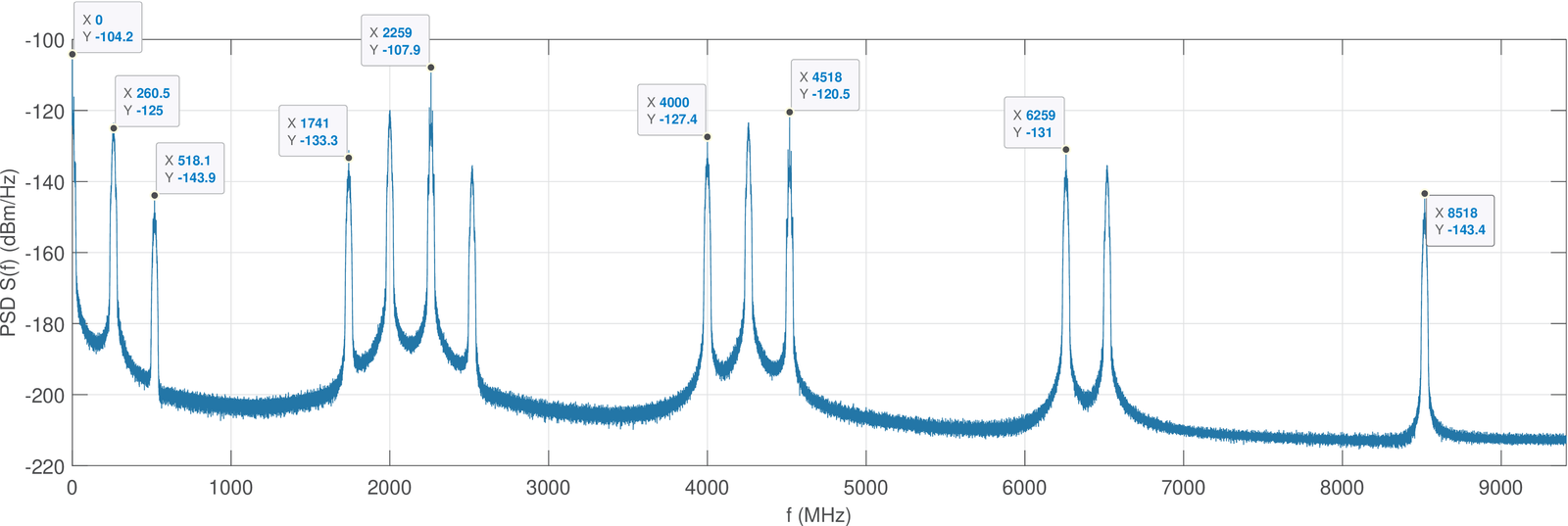
As indicated in Table 4.4, there is a factor of 4 between the signals associated to and (located in Figure 4.54 at frequencies 1.741 and 8.518 GHz, respectively), which corresponds to dB. This is confirmed by the difference of the respective PSD values (see the datatips in Figure 4.54): dB. Datatips for the DC and eight of the center frequencies are shown in Figure 4.54. With the exception of the datatip at 259 MHz (from ), all other eight parcels have a discrete line. In other words, among the 13 parcels in Figure 4.54, there are 5 that do not have a discrete line, and the one corresponding to 259 MHz is the only one with a datatip. This is better visualized by zooming Figure 4.54 as done in Figure 4.55. The results generated by the script ex_fftBasedQAMCarrierRecovery.m are SER equals to zero and EVM=1.9 %. Figure 4.56 shows the transmit and received constellations after carrier recovery. 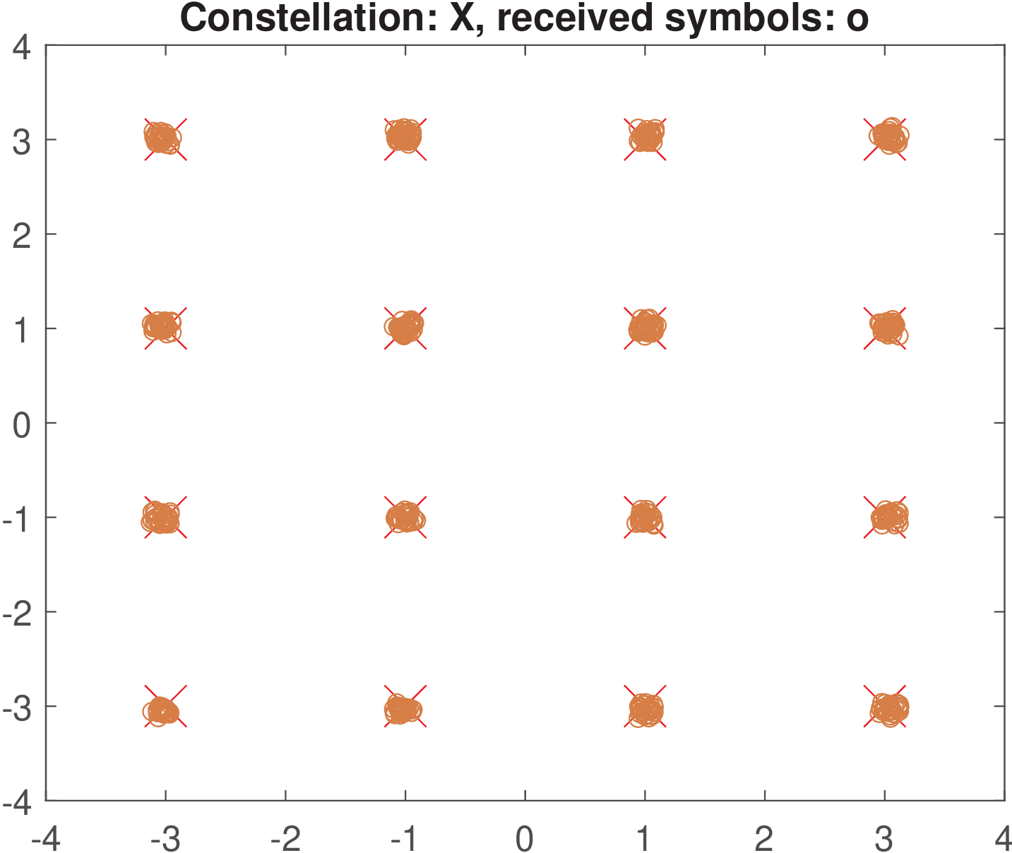
Different from the PAM case of Listing 4.19, where the estimated offset was obtained via a normalization by , the relation between the actual phase offset and the phase at the chosen FFT (of the signal) peak is more involved. One indication of this fact is that the signal of interest, related to in Table 4.4, is composed by both in-phase and quadrature components. To illustrate the issue, the script MatlabBookFigures/figs_synchronism_carrier_recovery.m generated Figure 4.57, which shows in its top plot the relation between (called fftPeakPhase in the script) versus . 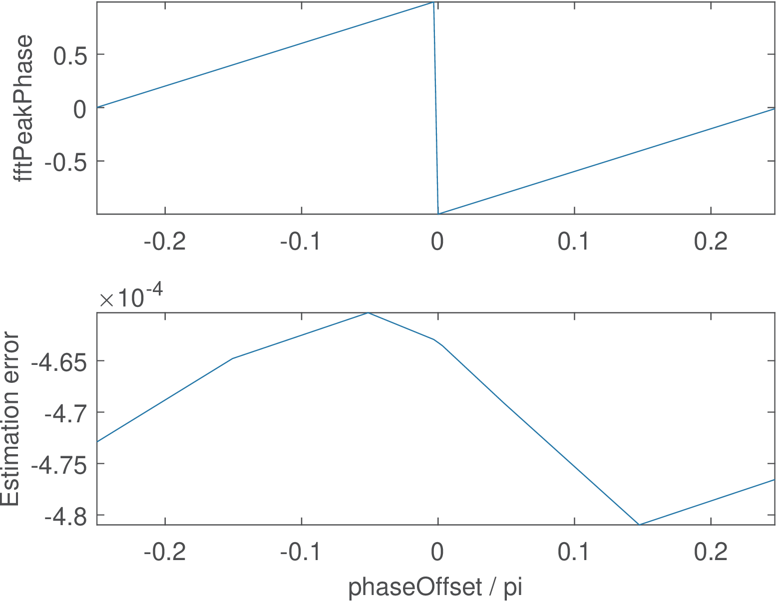
Listing 4.20 shows the lines of the mentioned script that specifically take care of obtaining the estimated offset (estPhaseOffset in the code) from , according to the top plot in Figure 4.57. 76[maxPeak,indexMaxPeak]=max(abs(R(1:maxIndexOfInterestInFFT))); 77fftPeakPhase=angle(R(indexMaxPeak)); %extract the phase at FFT peak 78if fftPeakPhase > 0 %deal with phase ambiguity assume offset is ... 79 estPhaseOffset = (fftPeakPhase-pi)/4; %in range [-pi/4, pi/4[ 80elseif fftPeakPhase < 0 81 estPhaseOffset = (fftPeakPhase+pi)/4; 82else 83 estPhaseOffset = 0; %avoid discontinuity at zero The bottom plot of Figure 4.57 shows the estimation error . Note that the abscissa range is . The FFT-based method used in Listing 4.19 (and ex_fftBasedQAMCarrierRecovery.m) is pedagogical but it is not used in practice due to its relatively high computational cost and the discussed limitations. The next section details the PLL, which is widely used in practice for synchronization purposes.
4.11.3 Phase-locked loop (PLL)As the name suggests, a phase-locked loop (PLL) is a closed-loop control system that generates an output signal with a phase that depends on the input signal phase . In other words, is said to be “locked” to because it is a function of the input phase. This relation typically corresponds to a time-delay such that or, for modeling purposes and without concerns with causality, a simple equality . Notice that keeping the phases in lock, implies that the frequencies are also locked. Some of the PLL applications are:
A typical PLL is composed of three main blocks: phase detector, filter and voltage-controlled oscillator (VCO). The PLL can be implemented in the analog or digital domain. A substantial fraction of the literature is devoted to the analog PLL. The digital PLL is, of course, closely related to its analog counterpart, but there are differences on their operations and even terminology. For example, the VCO in the digital PLL is often called numerically controlled oscillator (NCO). This discussion starts by the analog PLL and then concentrates on the digital version. As pointed out, the PLL is a versatile block and, therefore, used in many applications. There is a wide range of distinct PLL circuits and the name PLL denotes the whole family not a specific circuit. Besides, the PLL output signal depends on the application. For example, the PLL can output a sinusoid to be used on frequency downconversion in synchronous reception or can eventually already output the signal of interest (e. g., a demodulated FM signal). AK-TODO: finish this brief introduction on different types of PLL. In many cases the PLL generates a pulse train (square waveform) or sinusoid. The PLL can work with sinusoids at its input or digitally modulated signals at the baud rate. The digital PLL (DPLL) can use NDA (non-data aided). The digital PLL (DPLL) can use decision-directed schemes. The strategy is to discuss continuous-time for sinusoids. Then...
4.11.4 Continuous-time PLL for tracking sinusoidsThe behavior of a continuous-time PLL is briefly described in the sequel with help from Figure 4.58. 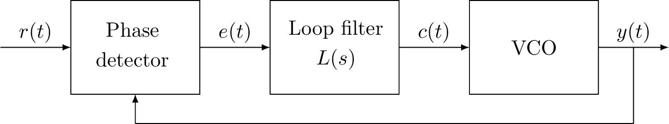
When the PLL is in “lock”, the VCO outputs a signal that is compared, by the phase detector with . The error signal is then used to drive the VCO to adjust to track . More specifically, the phase detector estimates the phase difference , where is the phase of the sinusoid generated by the PLL. This difference passes through the loop filter, which outputs a control signal that drives the voltage-controlled oscillator (VCO). To keep the PLL in lock, the error must be within a range, such as , which is called the lock range. Hence, the PLL operates in one of the modes: acquisition or tracking mode. There are special techniques to bring the PLL to its lock range, i. e., from the acquisition to the tracking mode. To make the discussion concrete and simple, it is assumed hereafter that the PLL outputs a sinusoid and that its input is , where is the noise. The PLL goal it to deliver a “clean” version
of . As mentioned, keeping the phases in lock, implies that the frequencies are also locked. Assume that , which can be modeled as . It is convenient to rewrite
where . This way, without loss of generality, the PLL treatment can assume that if a frequency offset exists, it is then incorporated in as a linear function of with slope . The next sections provide more details about the PLL components, assuming a sinusoidal phase detector. VCOBefore discussing the VCO, it is useful to recall that the instantaneous angular frequency of a sinusoid is simply the derivative
Inspired in Eq. (4.74) or Eq. (4.75), is assumed to be composed by a nominal frequency (in Hz) and time-varying phase and, from Eq. (4.76):
Now, it should be considered that the VCO has its oscillation frequency controlled by the input voltage . The actual relation between input and output can be nonlinear but it is often modeled as the linear relation
where is the nominal (or quiescent) linear frequency of the oscillator and is a gain (also called oscillator sensitivity). For simplicity, assume that , and compare Eq. (4.77) and Eq. (4.78) to obtain the control signal as
Hence, when used in a PLL, the VCO output phase is
such that the VCO output , as in Eq. (4.75), is controlled by . Phase detectorAmong many options, a phase detector can be implemented in continuous-time domain with a mixer and lowpass filter. One alternative is to use the trigonometric identity and, assuming , obtain at the mixer output
A lowpass filter is used to get rid of the term with angular frequency such that, ignoring the scaling factor , the output of the phase detector composed by the mixer and filter is when is sufficiently small such that . Similar to the variety of PLL circuits, there are many other phase detectors. Loop filterFrom a simplistic point of view, can be seen as a linear filter. However, because controls several important PLL features such as stability, settling time, etc., its study and design is based on control systems theory as discussed in the sequel. A linear model for the continuous-time PLL in the phase domainIt is convenient to perform a PLL analysis that does not depend on the signals amplitudes but only on their phases. This can be done in the so-called “phase domain”, where and are the input and output phases, respectively. Figure 4.59 represents a linear model that is suitable to design and analyze a PLL when operating in its linear range. 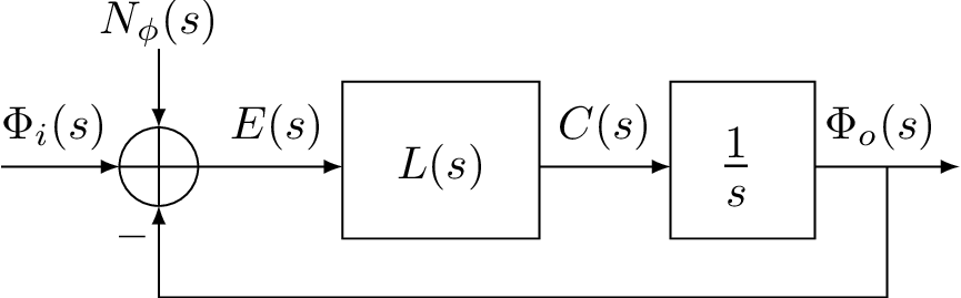
All signals in Figure 4.59 are represented using Laplace, with and being the transforms of and , respectively. is the Laplace transform of the signal , which is the PLL phase noise. In Figure 4.59, the integral of Eq. (4.80) is represented as . The PLL phase transfer function is defined as , with the assumption that . From Figure 4.59, and , such that
Similarly, it is possible to obtain the phase error transfer function as
It is useful to recall from control theory that a closed-loop with unitary feedback as in Figure 4.59 has a transfer function
where is the open-loop transfer function. Eq. (4.82) can be obtained from Eq. (4.84) because in this case . One alternative for the loop filter is
which corresponds to a PI (proportional-integral) controller. This option is called a second-order PLL given that Eq. (4.82) becomes a second-order system when is given by Eq. (4.85). Alternatively, using would correspond to a first-order PLL. The first-order PLL has a non-zero steady-state phase error when there is a frequency offset (difference between and ). Hence, due to its improved robustness, the second-order PLL is discussed in the sequel. Substituting Eq. (4.85) in Eq. (4.82) leads to
which corresponds to Eq. (E.31) when and . As indicated by Figure E.20b, the parameters and (or, equivalently, and ) can be tuned to obtain the desired behavior of the PLL. For example, a larger bandwidth (primarily controlled by ) implies in more phase noise at the output, given that has a wide bandwidth, but allows a faster tracking interval. The transient behavior of a PLL can be observed by assuming that the input is a step function and obtaining the step response associated to Eq. (4.86) (or, equivalently, Eq. (E.31)). Figure 4.60 illustrates the step responses for rad/s and four values of . 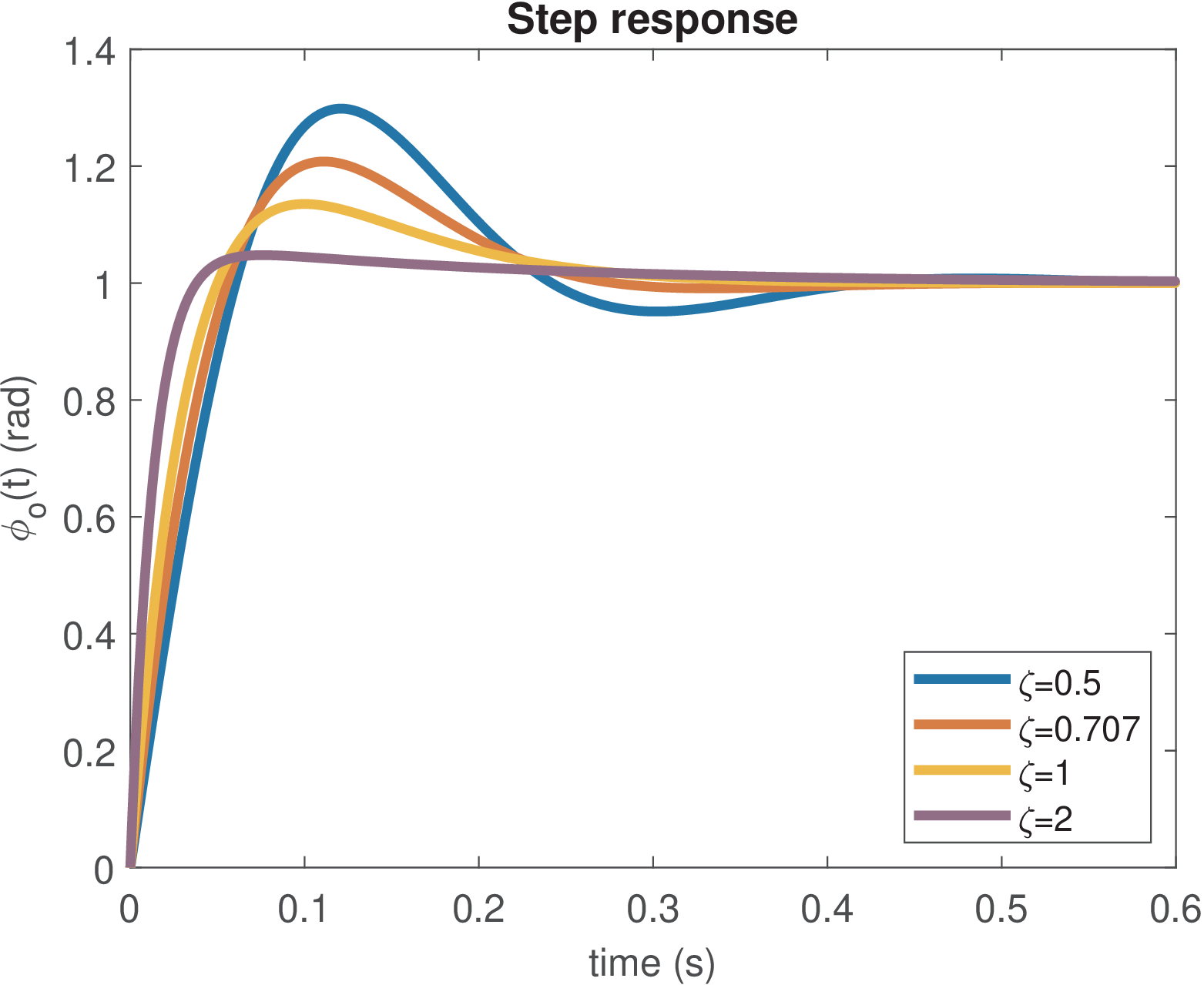
From Figure 4.60 it can be seen that a larger implies an improved tracking performance (faster and without overshoot) but a larger bandwidth, and consequently, output phase noise, as illustrated in Figure E.20b. Due to this tradeoff, is often used in practice. Example 4.25. PLL output when there is a frequency offset. Complementing the step response, the ramp response allows to evaluate the PLL when there is a frequency offset such that and . Because the assumed model is linear, the output will scale with any input scaling factor, and it suffices to adopt and use the ramp as input. Figure 4.61 depicts ramp responses for rad/s and two values of . It can be seen that the output presents a transient but then follows the input, which can be seen especially for . 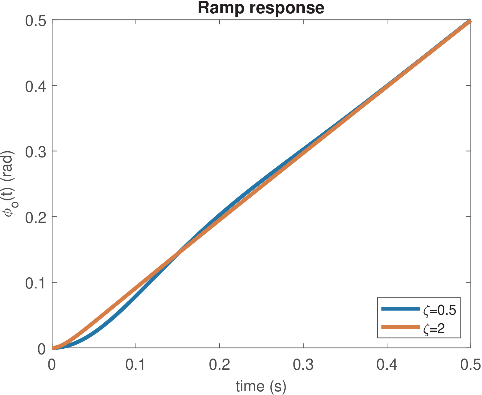
In complement to graphs of transfer functions as Eq. (4.82), it is illustrative to observe the phase error transfer function as in Eq. (4.83), which for the second-order PLL with given by Eq. (4.85), corresponds to Eq. (E.30). Figure 4.62 illustrates the PLL error for rad/s and three values of when the input is the same ramp as in Figure 4.61. 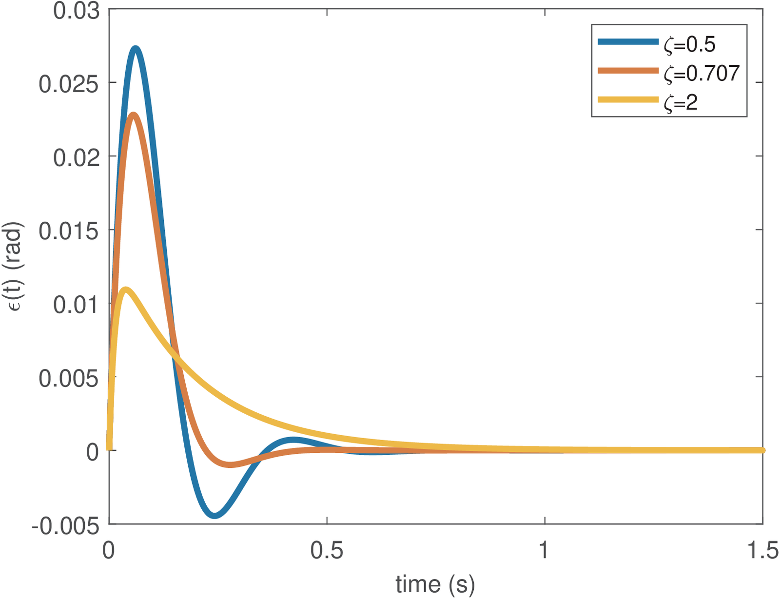
Recall that, when obtaining Figure 4.62, it was assumed . The values in Figure 4.62 should be scaled by when the goal is to determine the lock range, for example. To illustrate, consider the maximum error for in Figure 4.62 is 0.027 and that the error is restricted to . In this case, , which leads to a lock range given by Hz.
4.11.5 Discrete-time PLL (DPLL) for tracking sinusoidsAK-TODO: include phase detector from Miao, page 397, before or later here. The block diagram of a discrete-time PLL (also called digital PLL or DPLL) is depicted in Figure 4.63, where the VCO is sometimes called NCO, as previously mentioned. 
The PLL input and output in discrete-time are and , respectively. Similarly, the discrete-time version of Eq. (4.79) is , where the sampling period can be substituted by another value, denoted here as , such that Eq. (4.87) can be written as
and is a gain (or “learning rate”) that can be 1 or another value. AK-TODO: Livro [FB10] (e parece que [Mia07]) usa(m):
The Z-transform of Eq. (4.87) gives the transfer function
which plays the role of the integrator in continuous-time. A linear model for the discrete-time PLL in the phase domainFigure 4.64 describes a linear model that is a discrete-time version of the model in Figure 4.59. 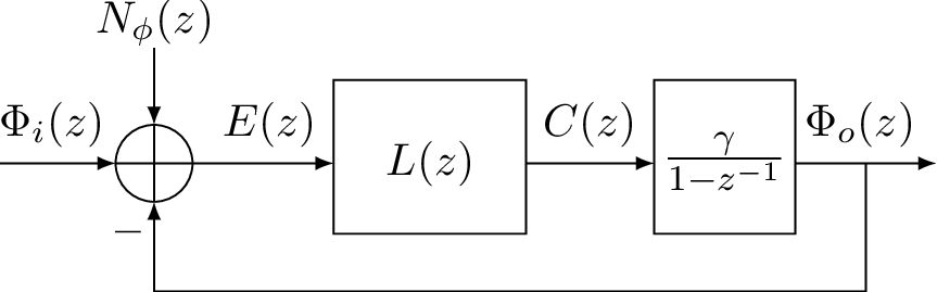
Assuming there is no phase noise (i. e. ) and from Eq. (4.84) with the open loop transfer function as , the transfer function is
A second-order DPLL is obtained with the adoption of
where and are the proportional and integral gains, respectively. Eq. (4.91) can be implemented according to the signal flow graph depicted in Figure 4.65. 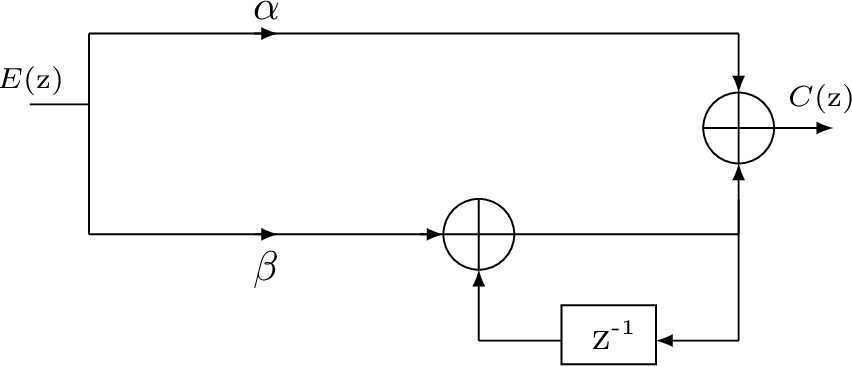
Using given by Eq. (4.91) and the integrator of Eq. (4.89) leads to the open loop transfer function22
Figure 4.65 can be obtained from Eq. (4.91) by adopting a parallel realization of , where and . The corresponding difference equation is , where and , which leads to
Other realizations can be developed by rewriting Eq. (4.91) as
which naturally leads to
The value in Eq. (4.95) is the previous output value23 and allows Eq. (4.95) to be implemented, e. g., as the transposed direct form II illustrated in Figure E.56 or any other standard realization. Incorporating Figure 4.65 into Figure 4.64 leads to Figure 4.66. 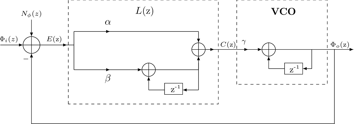
Substituting Eq. (4.94) into Eq. (4.90) leads to
4.11.6 Design of PLL and DPLLThere are several distinct options for implementing the blocks that compose a PLL. Hence, PLLs differ in many details. The reader is warned that AQUI and AQUI, for example, are only options among many alternatives.24 Design of continuous-time PLLA second-order PLL is assumed here. The loop filter is given by Eq. (4.85) and the VCO is modeled as . Hence, the PLL phase transfer function is assumed to be given by Eq. (4.86), which corresponds to Eq. (E.31). AK-TODO TO-DO - Hence, tabl sosParameters4 provides the relations among parameters of interest. Design of discrete-time PLL
4.11.7 Discrete-time PLL (DPLL) for tracking digitally modulated... decision directed...20 Note that this is valid for PAM, but not necessarily for QAM. As discussed in Appendix A.18.2, some QAM constellations lead to and a discrete spectrum component would not be created. 22 When a DPLL has a with all poles at as in Eq. (4.92), it is called a perfect PLL. 23 In contrast, note that in Eq. (4.91) is not an output value, but a parcel of the output . 24 For example, [NYHK94] thoroughly evaluates the model of a PLL used by NASA that slightly differs from the models discussed here. |